Reading the JEDEC spec so you don't have to.
Introduction
GPUs have an insatiable demand for data to calculate the next image. Textures, Z buffers, stencil buffers, color buffers etc. They are constant being read or written from and to memory.
As a result, one of the critical factors that determines GPU performance is external memory bandwidth: the amount of bytes that can be transferred per second between the GPU and the external DRAM.
After a steady progression in memory speeds, the industry had more or less stalled with GDDR5 running at a maximum speed of 7 Gbps per IO pin. The first GPU to be outfitted with this speed was the GeForce GTX 770, introduced on May 30, 2013. And that's where things seemed to end.
AMD took the radical approach of switching to HBM for their Fury GPUs, but with the high cost of stacked dies and interposer, there was an opening for an alternative.
On september 1, 2015, Micron made an under-the-radar pre-announcement of such an alternative:
In 2016, Micron will formally announce the launch of a new graphics memory solution with data rates targeting 10–14 Gb/s—an increase of up to 2X today’s mainstream GDDR5 speeds! Most importantly, this new product will remain in a traditional component form factor, similar to GDDR5, reducing the burden and complexity of design and manufacturing. Stay tuned for more updates on this exciting new graphics memory solution.
GDDR5X was born.
While officially unconfirmed, with up to 2 times the bandwidth of GDDR5, it's obvious that future GPUs will use this new memory standard, something that can easily be confirmed by some trivial google work:
Meanwhile, more information trickled out, and in November 2015, JEDEC standard JESD232 was published with the title "GRAPHICS DOUBLE DATA RATE (GDDR5X) SGRAM STANDARD".
Let's dive in, check out the details and see how it compares to GDDR5.
GDDR5X in a nutshell
The standard goes out of its way to mention that GDDR5X is very much built on and an evolution of GDDR5, and those who are familiar with the latter will feel right at home.
Here are some key points:
- QDR mode: data can be transferred at up to 4 times the rate of the word clock. (New!)
- Both QDR and DDR mode available. (GDDR5: DDR only)
- 16n prefetch (64 bytes per read or write) / burst length of 16 in QDR mode. (New!)
- 8n prefetch (32 bytes per read or write) / burst length of 8 in DDR mode. (Same as GDDR5)
- pseudo-independent memory accesses with 32 bytes (QDR) or 16 bytes (DDR) granularity. (New!)
- GDDR5 address compatibility mode.
- 1.35V supply for core and IOs. (GDDR5: 1.35V or 1.5V)
- 190 ball BGA package. (GDDR5: 170 ball BGA)
- memory sizes are defined up to 2GB per device. (GDDR5: up to 1GB)
The most important feature is the new QDR mode, but there are some interesting aspects about the other points as well. We'll have a deeper look at them below.
A Few Basics
To better understand what follows, here a quick refresher about the internals of a DRAM in general. What follows is true for all types of SDDR DRAM, LPDDR DRAM, GDDR DRAM, and even HBM.
Major Blocks & Bit Storage
Each DRAM consists of 3 major blocks:
- The memory core, where the bits get stored.
- The control logic, which is used for various maintenance operations.
- The interface logc, which is used to transfer data in and out of the chip.
The memory core has a hierarchical organization that looks like this:
- Each chip has a certain number of banks.
- Each bank has a certain number of rows. They're also called pages.
- Each row has a certain number of columns.
- Each column contains 1 atom of data.
- Each atom has a certain number of bits.
When you want to read or store data into a DRAM, you always have to do it by atom size.
The contents of each bit are stored in a incredibly tiny capacitor that can contain an electric charge (which represents a value of 1) or no charge (guess...).
A very important aspect is that checking the contents of this little capacitor results in a (very small) current that will empty its charge. In other words, a read operation is destructive!
Reading & Writing Data
To successfully access data in a DRAM, the following steps need to happen:
- For a particular bank, select one row that contains the data that you want to transfer. The correct terminology for this is to 'open a page'.
- copy over all the data from that row to a small static register (memory). The data in the main memory core has now been destroyed, but luckily you now have a copy of it somewhere else!
- Read or write atoms from and to as many columns as you want. In reality, you're accessing that small static register, of course.
- When you're done, copy the static memory back to its row location in the main memory core. This operation refreshes all the capacitors with new charges. You're now 'closing the page'.
Refreshing Data
Another important characteristics is that the capacitor isn't perfect: over time, the charge will leak away. To counteract this leaking, the contents of those little capacitors need to be refreshed periodically.
The control logic on the DRAM chip helps with that, but the memory controller of the CPU or GPU is still in charge of managing the overall operation.
The actual refresh itself is very similar to making a real access to the DRAM: select a row, read out its data, store the data back. In older DRAMs, the memory controller needed to keep track of which row to refresh when, but current DRAMs have an internal counter to just rotates from one page to the next. All the memory controller needs to do, is to stop data transactions to a bank every once in a while, issue a page refresh cycle, and continue with normal work.
Interesting fact: since regular data transactions also open and close a page, you could count that as a refresh. In theory, you could skip refreshing pages that have been accesses recently. In practice, this would only be a very minor optimization that's not really worth doing.
Quad Data Rate - QDR
The most striking new feature of GDDR5X is the addition of quad data rate.
In digital electronics, all transactions, internal and external, happen off a clock. The clock is a wire that continuously toggles between 0 and 1, and is used to ensure that all components on and off the chip operate in unison.
The vast majority of digital logic works on only the rising edge of the clock. This means that transaction only happen when the clock toggles from 0 to 1, and nothing happens when going from 1 to 0.
Initial SDRAM worked just like that: one word of data was transfered on the rising edge of the clock only, as illustrated in the drawing below.

While perfect for internal signals, there is an inefficiency associated with this: the clock signal will toggle at double the maximum possible data rate of the data. External high speed signals are restricted in their speed by the characteristics of the PCB material, the capacitance of the IO pins and so forth. For highly specialized wires like DRAM data pins, it's fine to add a little bit complexity on the sending and receiving end in return for a clock signal that runs lower.
And thus DDR was born: data bits now toggle both at the rising and falling edge of the clock.
QDR is taking this one step further.
4 data words are now transferred per WCK clock cycle.
An obvious question is whether or not there needs to be an internal clock that's double as fast as WCK to take in the data words that don't coincide with the rising or falling edge of WCK. The answer here is no: 4 different versions are created of WCK that are each delayed by an additional 1/4th of the total clock period of WCK. The result are 4 rising edged that are spaced evenly across the clock period, each of which can sample their respective data word.

Delay Locked Loop Primer
Since clock speeds are programmable, and delay elements on a chip have varying delays depending on temperature and voltage, a delay locked loop (DLL) is used create the 4 phases of WCK. The 3 key elements of a delay lock loop are a digital delay line, a multiplexer that selects one or more delayed versions of the input signal out of the delay line, and a phase comparator that check whether or not right delayed versions have been selected from the delay line.

In the figure above, the GPU generate or the DRAM receives from the GPU the original WCK. WCK enters a long delay line. The output of each delay element is fed into a large multiplexer. The first order of the control logic is the find the number of delay elements that's needed to match the length of the period of WCK. In other words, we're trying to create a signal WCK_FB such that it's rising edge coincides with the rising edge of WCK.
Let's say that there are 128 delay elements. Initially, the logic select an arbitrary delay element for WCK_FB, say, element 64. The phase compare block checks if the rising edge of WCK_FB comes before or after the rising edge of WCK. If WCK_FB is later, then too many delay elements were selected and the multiplexer is updated so that WCK_FB is created from a delay element ealier. If WCK_FB came earlier than WCK, the opposite happens. When the edges coincide, the DLL has locked onto the incoming signal.
We can now take the number of taps use to create WCK_FB, divide it by 4, and use those delays to create the different phases.
For example, 68 delay elements were needed to make WCK_FB match WCK, we'll use 0 elements for WCK_0, 17 delay elements for WCK_1, 34 elements for WCK_2, and 15 elements for WCK_3.
The control logic doesn't stop operating once the DLL has achieved lock: as temperature conditions change, the delay units may change as well, so it's best to keep on updating continuously.
QDR and DDR Mode
GDDR5X supports both QDR and DDR. Switching between the two modes is done by programming a bit in one of the DRAM mode registers.
It makes sense to keep a DDR mode around: it can save quite a bit of power.
In GDDR5, the presence of a PLL/DLL unit was optional: the RAM could use the rising and falling edges of WCK to capture or transmit the data from or to the GPU. A PLL/DLL can consume quite a bit of power, so it's nice if you don't need them. In practice, it's likely that all high speed GDDR5 devices have a PLL/DLL unit and that it is enabled when running the clock at top speeds, but it's also very likely that the PLL/DLL can safely be switched off when the clocks are much lower. For example, when the GPU is just sending out a static desktop.
With QDR, a rising and falling edge of the clock are not sufficient to capture all the data words on the bus, so the PLL/DLL is a necessity in QDR mode. But the low power cases still exist. That's when you went to switch off the PLL/DLL. As a result, a DDR mode is required.
16n Prefetch
What is it and why?
Prefetch is the concept where, for a particular data request, the DRAM doesn't return 1 word that's the size of the external data bus, but multiple one.
While you have a DRAM with a 32-bit wide data bus, a 2n prefetch size means that the DRAM will return 64 bits for each request for data. A 16n prefetch size means that each request will return 512 bits, or 64 bytes, of data.
Thanks to the concept of prefetch, the address and command busses, used to send or request data to and from the DRAM, don't need to run at a speed that's as high as the data busses. Another benefit is that the internals of the DRAM don't have to run at a very high speed, and that only the interface needs to run that high: when it receives the request, the DRAM can fetch all the 512-bits in parallel from one particular column address, and return the data in pieces to the interface. Without prefetch, the GPU could request a different 32-bit address at the highest speed, and, to keep up, the DRAM would have to operate at the same speed internally to return a different word.
So prefetch really has quite a bit of benefits.
In QDR mode, the prefetch size of GDDR5X is 16n, while DDR mode has a prefetch size of 8n. This makes sense: QDR is double the speed of DDR. By making the prefetch size double as well, the core of the DRAM can run at identical clock speeds for QDR and DDR.
The Bad News
So far, the everything that I've said about increased prefetch has been for the benefit of those who need to design and fabricate the GDDR5X chips. But what's in it for those who want to use them?
It's not as rosy there. In fact, I can only think about negative consequences!
For optimal performance, the memory architecture of a system needs to take into account the characteristics of the DRAM that is attached.
Take the cache of a CPU or a GPU: it would be incredibly inefficient to have a cache line size that is smaller than the prefetchs size of the DRAM that is attached to it. If your DRAM had a prefetch size of 32 bytes, and your cache line size had a prefetch size of 16 bytes, reading something from DRAM would require the replacement of of 2 cache lines. This is called cache line overfetch. Similarly, even if only 1 cache line were polluted, updating it back to the DRAM would require writing 2 cache lines as well.
For this reason, cache lines are rarely, if ever, smaller than the prefetch size of the external DRAM.
In the case of Nvidia GPUs, we find the following in the Global Memory section of the CUDA programming guide:
A cache line is 128 bytes and maps to a 128 byte aligned segment in device memory. Memory accesses that are cached in both L1 and L2 are serviced with 128-byte memory transactions whereas memory accesses that are cached in L2 only are serviced with 32-byte memory transactions. Caching in L2 only can therefore reduce over-fetch, for example, in the case of scattered memory accesses.
This suggests that at least some parts of the GPU memory system is designed for a 32 byte prefetch. The 64 byte prefetch may result in overfetch when filling up the L2 cache with data. This would reduce the cache hit ratio and reduce effectiveness of the memory bandwidth increase of GDDR5X.
(AMD's GCN Architecture Whitepaper states that they have an L2 cache line size of 64 bytes, so they should be good.)
The DRAM developers must have known that many existing memory systems are designed with a 32 byte prefetch in mind, so they came up with a partial solution. Which brings us to the next feature...
Pseudo-independent Memory Accesses
Up to now, everything has been relatively straightforward. But pseudo-independent memory accesses are a truely new feature.
Recapping from the earlier section about the basics, an access to DRAM requires opening a page in a bank, and selecting an atom from a column of that page.
This is shown in the picture below: both DQ[31:16] and DQ[15:0] are getting their data fromt the same column.
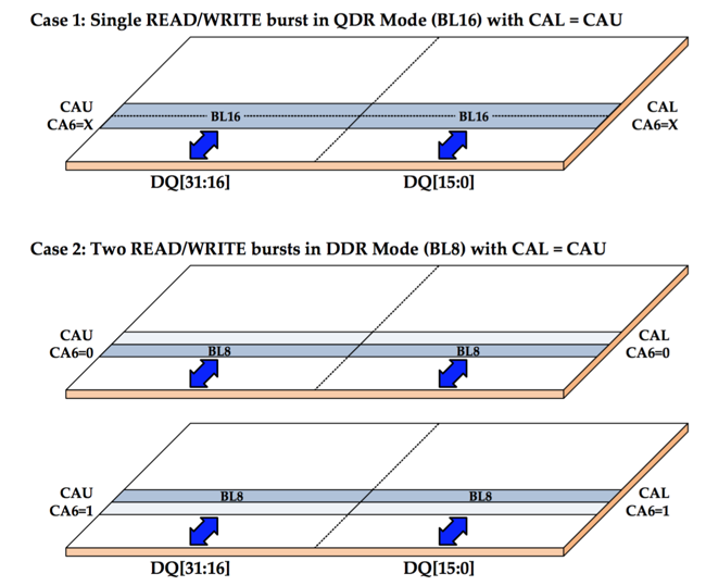
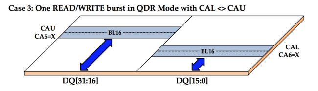
In GDDR5X, that is still possible (it's called Address Compatiblity Mode), but the default mode for both QDR and DDR splits up data bus into 2 half-sized busses. The lower half-size bus can select the the lower half of an atom from any random column within that page, while the upper half-size bus can select the upper half of an atom from any random column within the same page.
For QDR, things now look like this:
And for DDR, like this:
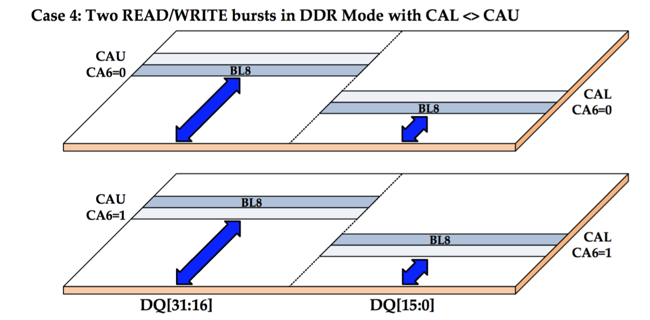
For QDR, the burst length is still 16, but since it's a half bus-width transfer, the total amount of data that is transferred is back to 32 bytes! Similarly, for DDR, the amount of data transferred is only 16 bytes.
As long as the memory controller can find transactions in the transaction queue that have 32 bytes sized atoms that come from the same page, it can now keep a cache line size of 32 bytes only, without having to suffer the efficiency loss that is caused by overfetch.
Of course, when it can not find a transaction within the same page, it has the option to either issue an overfetch, which could potentially reduce the efficiency of the cache. Or it could still only fetch 32 bytes, which would, for that transaction, reduce the bandwidth of the DRAM by half.
Looking back at the cache organization of Nvidia GPUs, the L1 cache line size is 128 bytes. If an L1 cache line needs to be fetched, it will automatically also fill up 4 L2 cache lines. So for those cases, there is not really a problem anyway. For data that only gets stored in L2, but not in L1, they will need to be smart about allocating that data such that there is a high chance that data from the same DRAM page gets used closely spaced in time.
I have little doubt that this will be the case in practice.
Why?
Because AMD is using 64 byte L2 cache line sizes! Worst case, Nvidia will simply fuse all its L2 cache lines pairs into one 64 byte cache line, and they'll be no worse off than AMD. Best case, there will be enough opportunies to match different columns from the same page, and they'll still enjoy the benefit of a 32 byte line size.
Minor Changes
1.35V Supply
GDDR5 allowed 1.35V or 1.5V that could be chosen independently for the core logic and IOs. With GDDR5X, it's 1.35V for both.
In addition to those power rails, there's also the pump voltage, Vpp, which is 3.3V for GDDR5 and 1.8V for GDDR5X. Vpp is used for some arcane transistor wizardy in the core memory, but that's about as far as my knowledge of these things go...
190 ball BGA Package
GDDR5 used to looks like this:
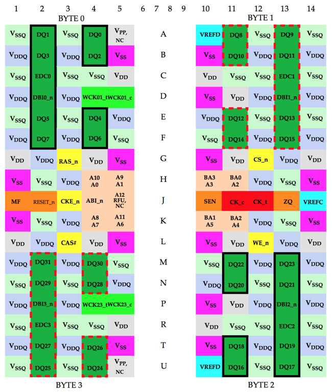
And GDDR5X looks like this:
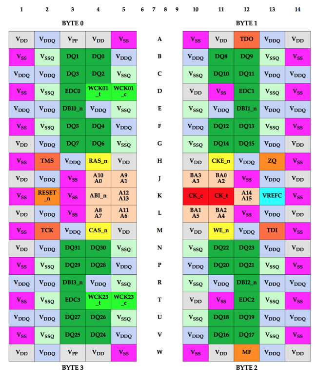
There are some ball movements, but they are minor. The biggest change is the addition of extra rows with power and ground at the top and the bottom rows. This is probably to better suppress voltage spikes that may happen due to the increased transfer speeds.
It's obvious that it won't be possible to create a sinle PCB to support both GDDR5 and GDDR5X chips. But in terms of PCB routing, the layout should be very similar.