Reading the JEDEC spec so you don't have to.
Introduction
Introduced with great fanfare last year by AMD, HBM is seen as the key to high performance GPU computing for the future. For the PC world, HBM is revolutionary in that it uses stacked dies that are mounted onto an interposer that also holds the main GPU die.
HBM reduces the data rate per IO from 7 Gbps per IO for GDDR5 to just 1 or 2 Gbps but more than makes up for it by increasing the number of IOs by an order of magnitude. The lower data rates and very short interconnection distances between the GPU and the DRAM remove the need for complex, high powered driver and high-speed sampler circuits.
Lower clock speeds and lower distance also require less agressive drive currents, and on-die termination resistors are gone completely. In combination with a lower power supply, this reduces the power consumption of the interface logic considerably, both on the DRAM and the master side.
AMD's Fury X and its derivates are using an early version, commonly named HBM1, that peaks at per-IO data rates of 1Gbps. With 4 so-called HBM stacks, that have 1024 data IO pins each, that's still good for a theoretical 512 GB/s.
But HBM1 is not a perfect solution:
- 512 GB/s, while fast, is only ~50% faster than a 7Gbps 384-bit GDDR5 bus. With GDDR5X on the horizon, that may not be sufficient for the future.
- Each HBM1 stack is only limited to 1GB, restricting practical implementations to a maximum of 4GB per GPU.
- A single vendor implementation, SK Hynix, with no public specification behind it, must be a bit costly.
Luckily, the big memory vendors of this world agreed to create an improved version, and propose it as an official specification.
The result is JEDEC Standard JESD235A - High Bandwidth Memory (HBM) DRAM).
After registering at the JEDEC website, the specification can be freely downloaded.
The standard uses the term 'HBM' only, with no references to HBM1 or HBM2, but to avoid any confusion, these terms will be used freely in this article.
It's probably not a bad idea to at least read up on the basics of DRAMs in general in the GDDR5X article. They won't be repeated here.
HBM2 in a nutshell
- Up to 8 independent channels per stack. Each channel is completely independent from the other.
- 128 data bits per channel.
- 32 byte atoms. Pseudo Channel Mode: burst length 4 at 64 bits/transaction. (HBM1, Legacy Mode: burst lenght2 at 128 bits/transaction.)
- IO pin redundancy for high packaging yield
- Optional data error correcting code (ECC) support per channel.
- One differential clock for commands, address, and data. (Unlike GDDR5(X), which has half rate clocks for commands and addresses.)
- Double data rate (DDR) for data and address bits.
- Page operations concurrent with reads and writes.
- 1.2V voltage rail for core and IOs
- All IOs are unterminated.
- Temperature dependent refresh rates
Multiple Independent Channels per Stack
In the GDDR5X article, we went through the basic organization of all current DRAM architectures, whether they're SDDR3, or GDDR5, or LPDDR. HBM is no different, but there's an additional hierarchical layer on top of it: an HBM stack is essentially the same as a bunch of independent DRAMs tied together. The name for each such independent virtual DRAM is called a channel.
Other than power and ground pins, and some shared reset and test pins, they really can be treated as completely separate from eachother: they each have a complete set of identical pins, they have asynchronous clocks, one channel can be operating while the other is in self refresh sleep mode, and so forth.
Each channel has following IOs:
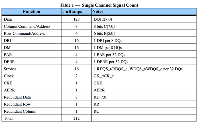
Since there are 128 data bits per channel, and up to 8 channels per stack, the maximum amount of data IOs per HBM stack is 1024.
1024 is the number that's quoted everywhere in the press, but it's interesting to note that versions with a smaller number are valid as well. That said, since bandwidth is the marquee feature for HBM, one wonders if there's a point to having versions with a lower number of IOs. After all, the bandwdith of a stack with 4 channels instead of 8 could be matched with a cheaper GDDR5X solution.
We'll dig a bit deeper into some of the IOs later on.
Another interesting tidbit is that vendors have complete freedom with respect to architecting where the channels will reside. We know from the Hynix HBM1 chips that each of the 4 dies in a stack has 2 channels, for a total of 8 channels, and that there is a 5th die at the bottom of the stack that has control logic. But if a DRAM vendor wants to do it differenlty, it can. The extra die is entirely optional, and the control logic may be implemented onto the DRAM core dies instead.
It's also possible to spread the memory of one channel across multiple dies of the stack, as long as the latencies for various operations are constant for all elements of the same channel.
Pseudo Channel Mode
The HBM specification document lists 2 modes of operation: legacy mode and pseudo channel mode.
A device can support one or the other, but not both. The memory controller can know which mode is supported by reading some bits in the DEVICE_ID register. It isn't stated explictly, but it's obvious the legacy mode corresponds to HBM1 and pseudo channel mode to HBM2.
In legacy HBM1 mode, each read or write transaction transfers 256 bits in a burst that consists of 2 cycles of 128 bits each. In pseudo-channel HBM2 mode, the 128-bit bus is split into 2 individual 64-bit segments. On each segment, a read or write transaction transfers 256 bits as well, but in a burst that lasts 4 cycles (of 64 bits each).
The pseudo channel concept essentially divides the memory of a single channel in half and assigns each half to a fixed pseudo channel.
Note that pseudo channel share the same address and command bus: you can send a command and adresses to one pseudo channel or the other, but not to both.
The immediate question is: how does that of any help?
As explained in the GDDR5X deep dive, pseudo channels were a way to still have 32 byte atoms instead of 64 bytes (though with same page restrictions). But this is not the case here since the atom is 32 bytes for both modes. In legacy mode, you get the 32 bytes of the full 128-bits bus in 2 cycles. In pseudo channel mode, you get 2 independent 32 bytes in 4 cycles. Pseudo channels actually increase the latency for a transaction from 2 to 4 cycles, and they also require the memory controller to issue 2 request instead of just 1 to keep the full 128-bit bus occupied.
The JEDEC spec doesn't provide any justification, but the answer can be found in a MemCon 2014 presentation by Hynix:
Pseudo channels improve tFAW by 60% compared to DDR4" and by 40% compared to HBM1.
This needs some explanation!
According to a blog post on Micron's website:
The four-bank activation window or tFAW is the amount of time in which ACTIVATE commands to four different banks can be issued.
Let's now go back to the JEDEC spec and see what they have to say about that:
There is a need to limit the number of bank activations in a rolling window to ensure that the instantaneous current supplying capability of the device is not exceeded. To reflect the short term capability of the HBM device’s current supply, the parameter tFAW (four activate window) is defined: no more than 4 banks may be activated in a rolling tFAW window.
The activate refers to opening a page in a bank. Opening a page in a bank copies data from the memory core to a small internal static memory (the sense amplifiers) from which the real read and write transactions happen. This copy operation costs power. To ensure that peak power stays in check, there is a limit to the rate by which activates are allowed.
Once 4 bank activation have passed, no more activations are allowed until tFAW (which started with the first activation) has passed. If the memory controller can schedule multiple transactions to the open pages, this is not a problem, since it will take longer than tFAW to complete those transactions. But if not, then the memory controller will have to go idle before it can schedule the next transaction. That's definitely bad to reach peak bandwidth.
In legacy mode, each page has a size of 2KB. In pseudo channel mode, it's only 1KB. The larger the page size, the larger the amount of power that's needed to open a page. Since psuedo channel pages are only half the size, it also requires roughly half the current.
Hynix goes on to to replace tFAW by tEAW: Eight Activate Window, where tEAW has the same duration as tFAW. The JEDEC spec sticks to tFAW term, but tFAW is just much smaller in psuedo channel mode than what it would have been for legacy mode.
In waveforms of their MemCon 14 presentation, legacy mode looks like this
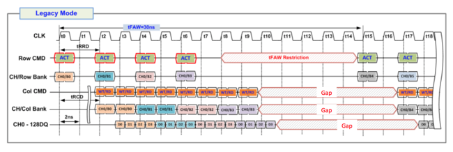
After opening 4 pages in different banks (ACT), and 2 tranactions to each page, the memory controller has to wait until tFAW expires.
Meanwhile, in pseudo channel mode, you get this:
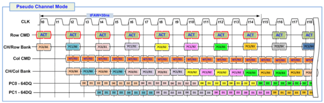
In this case, 8 pages are opened in different banks, and by the time all transactions are complete, tEAW has expired and new pages can be opened.
It's clear that pseudo channels will dramatically improve bandwidth for this particular case, but whether or not this kind of improvement can be seen in the real world depends on the traffic patterns that are being present to the memory controller.
There's still a lingering question: was it really necessary to have pseudo channels to reduce tFAW? Why not just reduce the page size of legacy mode and be done with it?
Interconnect Redundancy Mapping
With the amount of pins that can exceed 1700, and up to 9 dies that can be stacked on top of eachother, and 4 (or more?) of those stacks that are mounted on onto an interposer, packaging yield should be a major concern.
That's why the row bus and the column bus of a channel each have a redundant pin, and a configuration register to remap pins around a single broken one. For the data bits, either the DBI pin or the redundant pin are used in the same way.
Busses can be repaired temporarily or persistently: in the former case, the memory controller needs to reprogram the repair registers at every power cycle. In the latter, the registers are permanently programmed with fuses. This is an unreversible operation that can only be performed once.
The programming happens via a serial test access port, IEEE Standard 1500, that's completely separate from everything else. This makes sense: a broken bus would make it very hard to program the repair registers!
Data Error Correction
A really interesting feature for HBM2 is the support for data error correction.
GDDR5 already supports data error detection, but it's limited in scope:
- per 9-bit channel (8 bits + 1 DBI bit) and over a burst of 8, so over a total of 72 bits, the DRAM calculates an 8-bit ATM-8 HEC checksum.
- The checksum is transfered back to the memory controller bit-by-bit via a dedicated EDC pin.
- The memory controller compares the calculated checksum against the received checksum.
- If there's a mismatch, the memory controller may decide to retry the operation.
It's very simple, and only allows detection of data transfer issues. Bit flip errors that happen inside the memory core itself cannot be detected.
With HBM2, for each 128 bit atom of data, the device can optionally store 16 additional bits of error correcting codes. The device doesn't have any functionality to correct or detect errors: that's entirely up to the memory controller to implement. To the DRAM, it's just extra storage.
The 16 bits are being transferred via the data mask (DM) IOs. Just like other DRAM types, HBM has one data mask pin per 8 bits of data pins. This pin is traditionally used to tell the DRAM whether or not a particular byte in memory must be overwritten during a write operation. That's also true for HBM by default, but when ECC mode is enabled, the pin gets repurposed and data masking is disabled.
Since ECC mode requires extra storage, one would expect this feature not to be present for HBM devices that are targeted for consumer applications.
In addition to data error correction, HBM also has parity checking for row address, column address, and data bits: the DRAM simply reports back whether or not there was a parity error, but it will still execute the operation if a parity error was detected. This reduces the usefulness to report a catastrophic failure only: who knows what command, address has really been executed, or what data was written when one of the bits was flipped!
Page Operations Concurrent with Reads/Writes
Or, as written in the spec, "Semi-independent Row & Column Command Interfaces allowing Activates/Precharges to be issued in parallel with Read/Writes".
What does this mean?
In almost all PCB mounted integrated circuits, IO pins are a highly sought after commodity: there are never enough of them. To reduce the number of IOs, a common practice is the map multiple functions onto the same pins.
In the case of GDDR5 and GDDR5X, there are 3 command pins (RAS_n, CAS_n, WE_n) and 9 or 10 address pins respectively. The 3 command pins allow for 8 different commands, but the most important ones are ACTIVATE (open a page), DEACTIVATE/PRECHARGE (close a page), READ, and WRITE.
For page operations, where RAS_n is asserted, the address pins are used to transfer the bank number and the row within that bank. For read or write operations, where CAS_n is asserted, the address pins are used to transfer the bank number and the column number, which select a specific atom within the page that was activated earlier.
Since it can take quite a bit of time to open or close a page, to achieve maximum bandwidth it is extremely important to interleave read and write operations from a page of one bank with opening and closing a page in another bank. But since the address pin are being used for both, the memory controller will sometimes have to choose between one or the other. In the end, that can reduce average bandwidth. (At least, that's the theory. Let see further below!)
With HBM, this is not the case: there are 8 dedicated columns IOs and 6 dedicated row IOs.
For row commands like ACTIVATE, it takes 2 double data rate clock cycles to transmit the row information, so that good for 24 bits to transfer bank number, row number, and some parity bits. Column commands like READ or WRITE, only takes 1 double data rate clock cycle, good for 16 bits, to transfer the bank number, the column number, and some parity bits.
With this arrangment, in legacy HBM1 mode, the memory controller can issue new reads or writes at a rate of 1 command per clock, and receive or transmit the 256-bit atom that goes with it at the same rate, all while opening or closing pages in other banks in parallel.
For pseudo-channel HBM2 mode, where a data transfer takes 2 clock cycles (burst length 4 at DDR), it can now issue double the commands than are needed to saturate one pseudo-channel, but since it will need to keep 2 pseudo channels busy, it will need to issue read or write commands in alternating fashion to keep those 2 pseudo-channel fully occupied as well.
All this sounds fantastic, and looks like a great improvement over GDDR5(X), but is this really true?
In GDDR5, data is transfered with a burst length of 8. Since the data clock is double the command clock (contrary to HBM, which has only 1 single clock), this corresponds to a burst length of 4 in a command clock time. And since it's DDR, that corresponds to 2 command clock cycles. In other words, you can saturate the bus as long as you are able to issue a read or write command every other command clock cycle.
This is illustrated in the following diagram from the GDDR5 JEDEC specification:
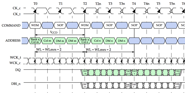
At T0, you see the first WDM (Write Data Mask) operation on the command bus, with the corresponding data being sent on DQ starting a T2. At T2, you see the second WDM operation with corresponding data starting at T4. There are no idle cycles on the DQ bus between the first and the second write.
However, we do see a NOP command on the command bus at T1! This NOP command could just as well have been used to issue an ACTIVATE command to open a page in a different bank.
What this illustrates, is that being able to issue row and column commands in parallel for HBM is not as much of a big deal as it initially seems: it is really a necessity due to the fact that the burst length of HBM1 is only 2. There may be cases where it still offers some performance benefits, but if so, the overall benefit is probably minor.
It's interesting that initial leaked Hynix slides featured the separate row and command busses quite prominently, but they aren't even mentioned in the Hynix slides that were presented at MemCon 14. Coincidence or not?
Signalling
For very high speed signals that travel over longer distances, think DRAM on a PCB, you need to treat signal wires like analog transmission lines. To prevent reflection, impedance jumps need to be avoided. This is accomplished by having termination resistors at the receiving end of where a signal is going.
Resistors on silicon are a bit of pain to deal with: they are often not very accurate, they take area, they also consume power.
Since the IO data rates of HBM are much lower, and the distances much shorter as well, termination is not required, so those negative aspects can be avoided. As result, the area that's taken up by HBM IOs should be quite a bit smaller than those taken up by traditional DRAMs.
In GDDR5(X), the extremely high speeds also require the presence of a PLL to create a stable clock to sample the incoming data bits as accurately as possible. The HBM spec doesn't mention the use of PLLs at all. That's another area of simplication and reduced power consumption.
2Gbps is still quite high, so a training sequence is still requires to ensure that IOs are sampled right at the moment where the signal the most stable.
Temperature Dependent Refresh Rates
The leakage of the DRAM cells go up with increasing temperature. Since refresh operations reduce bandwidth, it makes sense to adjust the refresh rate accordingly. HBM has a few pins that tell the memory controller at what rate it is supposed to refresh its content.
This is dfferent from GDDR5, which allowed a memory controller to read back the temperature without instructing exactly which refresh rate was appropriate.
Some HBM devices have a catastrophic temperature sensor as well: if the transistor junction temperature of any die goes above a limit, it will inform the memory controller.
Conclusion
HBM2 is a very exciting technology. It's fast, it's lower power, it's very compact.
It's not perfect, cost is the biggest question mark, but 2016 should be the year were we start seeing a couple of products that use it: Nvidia has already confirmed its usage for Pascal, AMD will probably follow suit with a FuryX successor. There are even rumors of AMD CPUs that will use HBM2 as well.
I hope you liked my reading of the HBM2 spec. For comments, corrections, questions, feel free to contact me at moninsider@gmail.com. You can also discuss it on Hacker News.
Revision History
Feb 2, 2016: first version