Reading the JEDEC spec so you don't have to.
Introduction
Things have been going fast in the DRAM memory world in the past two years. In June 2015, AMD released the Fury X GPU, the first product with HBM memory. Less than a year later, Nvidia followed up with the P100 GPU, the first one with its faster brother, HBM2. And just a few months later, Nvidia announced the GTX 1080 GPU, the first product to use GDDR5X.
At the time of this writing, there are GPUs on the market that run GDDR5X a staggering 12Gbps per data pin.
Could we possible want or need more?
Of course, we do!
While an official JEDEC standard, GDDR5X was clearly a detour, supported only by Micron, on the way to greater things. At the Hot Chips 2016 conference, Samsung first talked about the successor, creatively named GDDR6. The official JEDEC specification, JESD250, was published in July 2017 with the following title: "GRAPHICS DOUBLE DATA RATE (GDDR6) SGRAM STANDARD". The images below were copied from the specification.
It speaks for itself that GDDR6 will be faster than GDDR5 and GDD5X, but are there other interesting changes lurking in the background as well? Let's find out!
GDDR6 in a nutshell
GDDR6 is an interesting melange of GDDR5, GDDR5X, and even HBM2 features.
If you only have 1 minute to spare, just remember the following points:
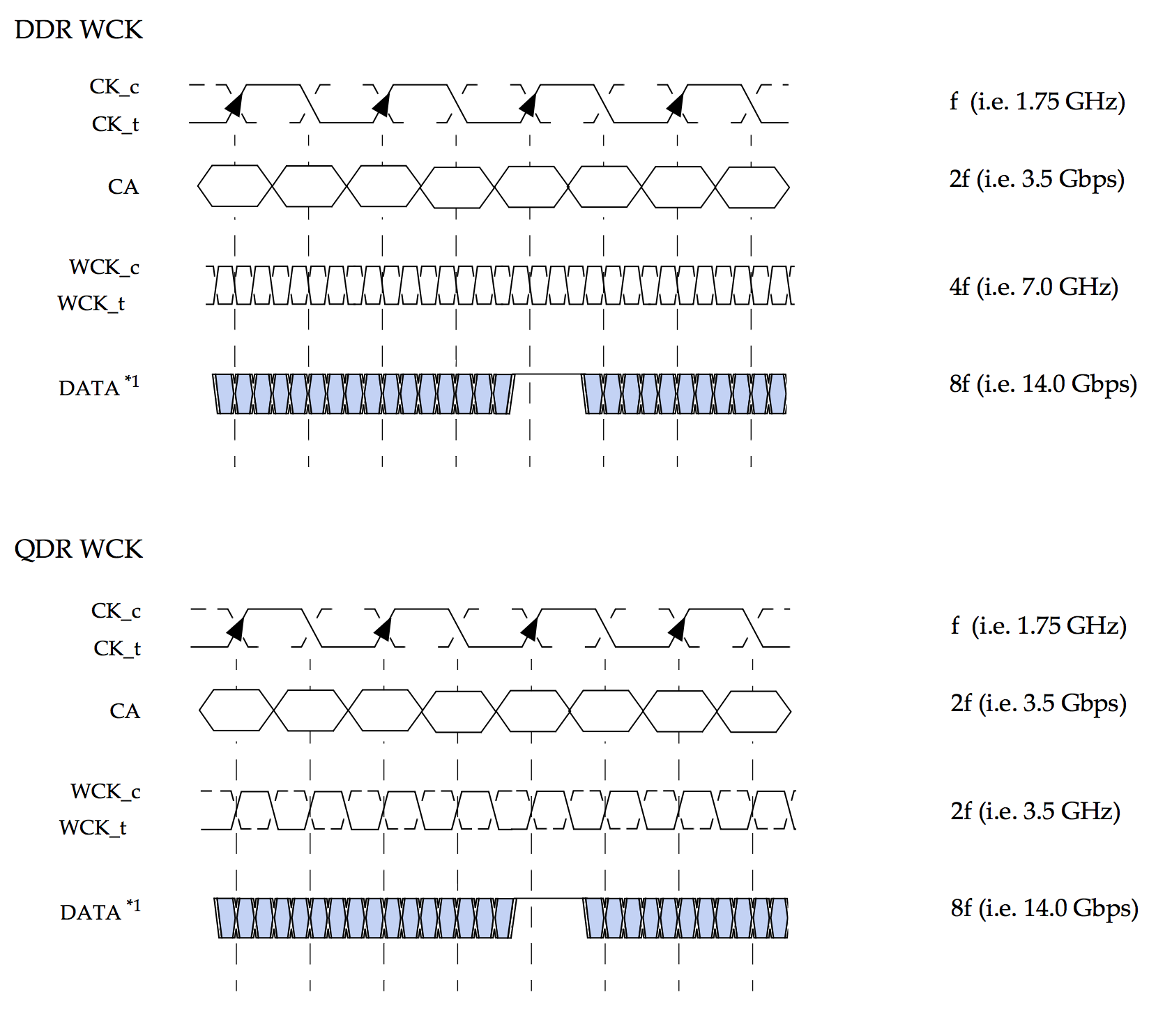
- Both DDR and QDR are possible with respect to the word clock. Vendor dependent. (DDR is similar to GDDR5, QDR is similar to GDDR5X.)
- 2 completely independent 16-bit channels. (Similar to HBM2)
- 16n prefetch architecture (32 bytes per read or write per 16-bit channel) / burst length of 16
- 1.35V supply for core and IOs. (Same as GDDR5X)
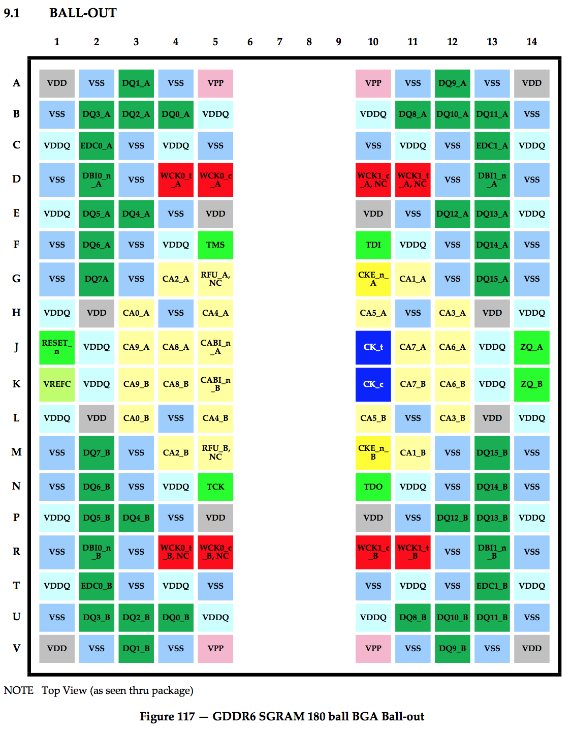
- 180 ball BGA package. (GDDR5: 170, GDDR5X: 190)
- memory sizes defined for 1GB, 1.5GB(!), and 2GB per chip, with placeholders in the spec for 3GB and 4GB. (GDDRX5: 1GB and 2GB)
- 16 banks (GDDR5: 8 or 16 banks, GDDR5X: 16 banks)
Two Independent 16-bit Channels
GDDR5 and earlier support 1 32-bit channel: it has one command/address bus, and one 32-bit data bus. It's simple and straightforward.
GDDR5X is more complex: it really only has one true 32-bit channel, but that channel can be split into 2 16-bit pseudo-channels. There isn't a whole lot of flexibility in this configuration since read and write operations for the pseudo-channels need to happen within the same row. That is: when accessing data from a particular row, the upper 16 bits can be used to transfer data from a different column than the one of the lower 16 bits.
HBM has truly independent channels: a single HBM stack behaves like a collection of completely independent DRAMs. There can be up to 8 truly independing channels per HBM stack, and each of those channels can be split ever more into 2 psuedo-channel that can access different columns and rows.
GDDR6 is like HBM: you have 1 chip, but it behaves like 2 fully independent DRAMs, with their own command/address bus and their own 16-bit data bus.
(One very minor difference between HBM and GDDR6 is the GDDR6 has a shared clock. This is not the case for HBM, but, in practice, it is very unlikely that an HBM memory controller would use different clock speeds for different channels.)
The more channels there are in a system, the more opportunitie there are for the memory controller to manage the DRAMs such that large stalls are avoided due to a page refresh, page activation limits etc. It's a feature where HBM really shines. Having two channels instead of one per DRAM helps in closing that kind of gap.
There is another very good reason why having two channels is crucial: it counteracts consequences of a 16 cycle burst length.
As discussing in detail in the GDDR5X article, having a burst length of 16 in combination of a 32-bit wide bus results in a transaction atom of 64 bytes. A lot of CPU and GPU architectures use transaction atoms of 32 bytes. By splitting up the DRAM into 2 independent channels of 16 bits, the DRAM designers can use a 16n prefetch while keeping the system architects happy with a transaction size of 32 bytes!
DDR and QDR
For the longest time, DRAM has been double data rate (DDR), with the data bits changing at the both the rising and the falling edge of the word clock (WCK). The advantage of DDR over single data rate (SDR) is that no part, not even the clock, on the PCB need to toggle at a faster rate than data bits themselves. It also still makes it possible to design the DRAM without an internal PLL/DLL at all, or with the PLL/DLL powered off.
GDDR5X introduced quad data rate, or QDR. With QDR, data toggles at 4 times the WCK frequency (which means that it toggles at twice as fast.) A PLL/DLL will always be required in this mode. GDDR5X supports both a QDR and a DDR mode, but during that DDR mode the DRAM runs at half the speed. In GDDR5X, DDR mode only exists as a low performance power saving option.
GDDR6 is the first DRAM where the DRAM vendor can decide to support either QDR or DDR at full speed. The specification does not require a vendor to support both. In a way, GDDR6 is really two standards!
By way of example: for a GDDR6 DRAM that runs at 14Gbps, WCK will run at 7GHz for a DDR device, and at 3.5 for a QDR device. (In both cases, CK, the command and address clock, will run at 1.75GHz, with command and address lines themselves running at 1.75Gbps as well.)
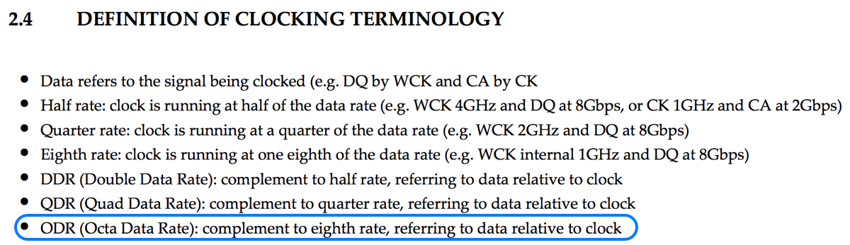
ODR?
Section 2.4 "Definition of Clocking Terminology" of the JEDEC specification doesn't only define DDR and QDR, but also ODR: Octa Data Rate. Unfortunately, there is no further mention of ODR in the rest of the spec, but could this be an unintentional hint of things to come? GDDR7 anyone?
Storage Capacity
Up to now, the storage capacity of all memory chips has been a nice, clean power fo two, if you exclude error detection or correction bits.
GDDR6 breaks with that tradition and offers in-between options. The standard allows a capacity of 8 to 32 Gbit, but 12 Gb and 24 Gb are possible as well. This will probably make GPU makers happy since it will increase the ability to segment the market based on the amount of memory.
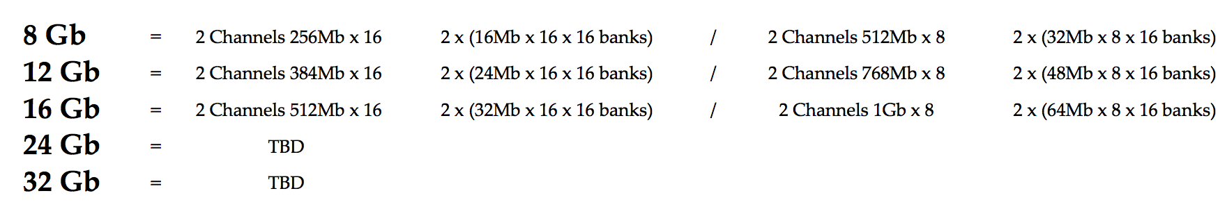
Right now, the exact bank configuration of the 24 and 32Gb versions hasn't been filled in yet, but sufficient pins have been allocated to support it.
Today, a GPU with a 256-bit bus can only cleanly support 4GB, 8GB or 16GB. With GDDR6, they will also be able to support 12GB, while still maintaining a full balanced load with identical sized memories connected to each controller.
Pseudo-Channel Mode
GDDR6 has a mode where a number of pins of the 2 channels are shared. This reduces the number of command/address pins one the side of the memory controller.
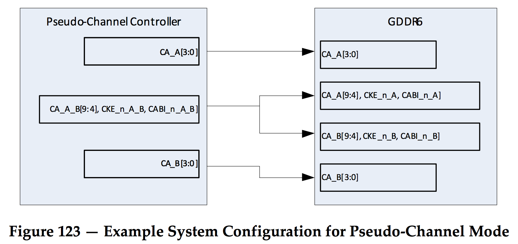
For a chip with a 384-bit memory interface that uses 12 GDDR6 chips, pseudo-channel mode would reduce the amount of IOs by 96. That's a considerable amount.
Among the shared pins are command/address bits CA[9:4].
The disadvantage is that this mode imposes significant restrictions on the way banks, rows, and columns can be selected between the two channels.
For example, for row activation, bits CA[9:4] are used to specify the 4 bank bits as well as 6 up to row bits. The memory controller will only be able to independently chose 7 of a maximum of 13 row bits. Luckily, the column bits can still freely be selected per channel.
Of course, since GDDR5X pseudo-channels require all row bits to be identical, a much tougher restriction, this is not deal breaker in any way. For very large chips, GPU makers may decide that the additional restrictions are a worthwhile tradeoff.
x8 - Clamshell Mode
GDDR5 made is possible to use only half of the data bus, 16-bits instead of 32-bits, while still being able to access all memory on the chip.
Similarly, GDDR6 has an x8 mode where only 8 of the 16 data bits are connected to the device.
Using this mode, one can connect 2 8-bit channels of 2 different GDDR6 devices to a single 16-bit channel on the controller.
The net result is a doubling of the maximum amount of memory that can be connected to the same memory controller.
In the picture below, you see how that works: on the left, you have standard single device x16 mode, with 2 16-bit channels per GDDR6 that are each connected to a channel controller.
On the right, you have 2 GDDR6 devices in x8 mode: each 16-bit channel is connected to two GDDR6 devices. The CA pins of a channel controller are going to both GDDR6 devices.
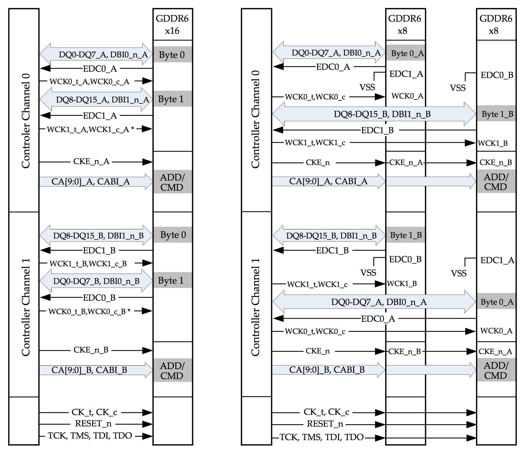
This kind of mode has traditionally been used for GPUs that have a lot of memory, such Nvidia Quadro and Tesla, or AMD FirePro products.
180 ball BGA Package
The number of balls on the GDDR6 BGA falls in between those of GDDR5 and GDDR5X. If you compare against the ballout of those two, you'll notice an increase in the number of command and address pins. That's a consequence of the fact that GDRR6 now has two independent channels.
Conclusion
GDDR6 isn't revolutionary. It has the usual increased capacity, and increased bandwidth. But the dual-channel feature is unexpected, and really nice for workloads with a lot of parallel reads and write to different parts of memory.
Revision History
December 16, 2017: first version